
 KAPSA Semicon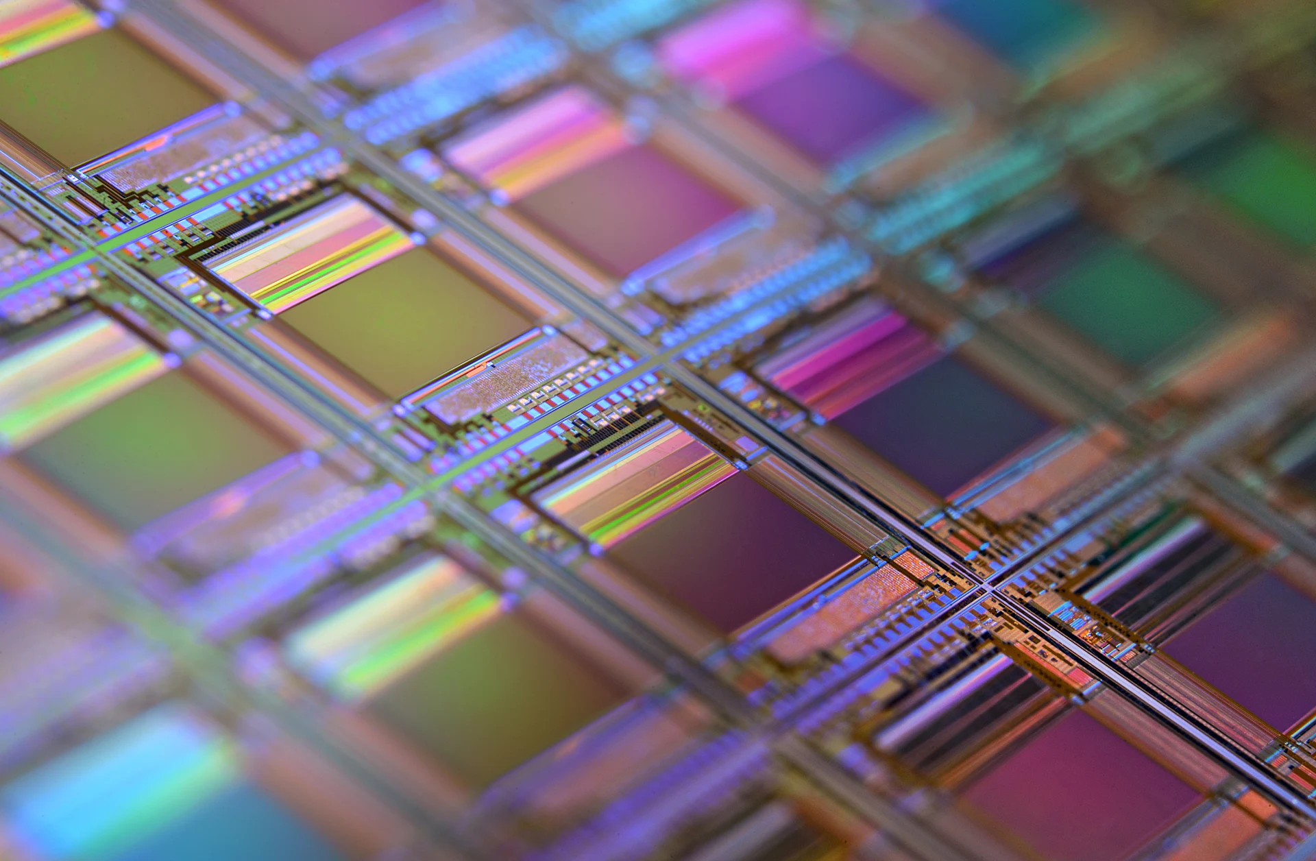
Beneath the Brain. Beyond Reliability.
Proving every chip is built to last.
Independent semiconductor testing, reliability qualification and failure analysis — from the wafer to the finished product — for India's fast-growing semiconductor and electronics industry.
- Wafer test
- Package test
- Burn-in
- Parametric test
- HAST
- THB
- Thermal cycling
- HALT
- SEM / FIB
- X-ray inspection
- Acoustic microscopy
- Decapsulation
- EMC / EMI
- XRD · XRF · FTIR
- Calibration
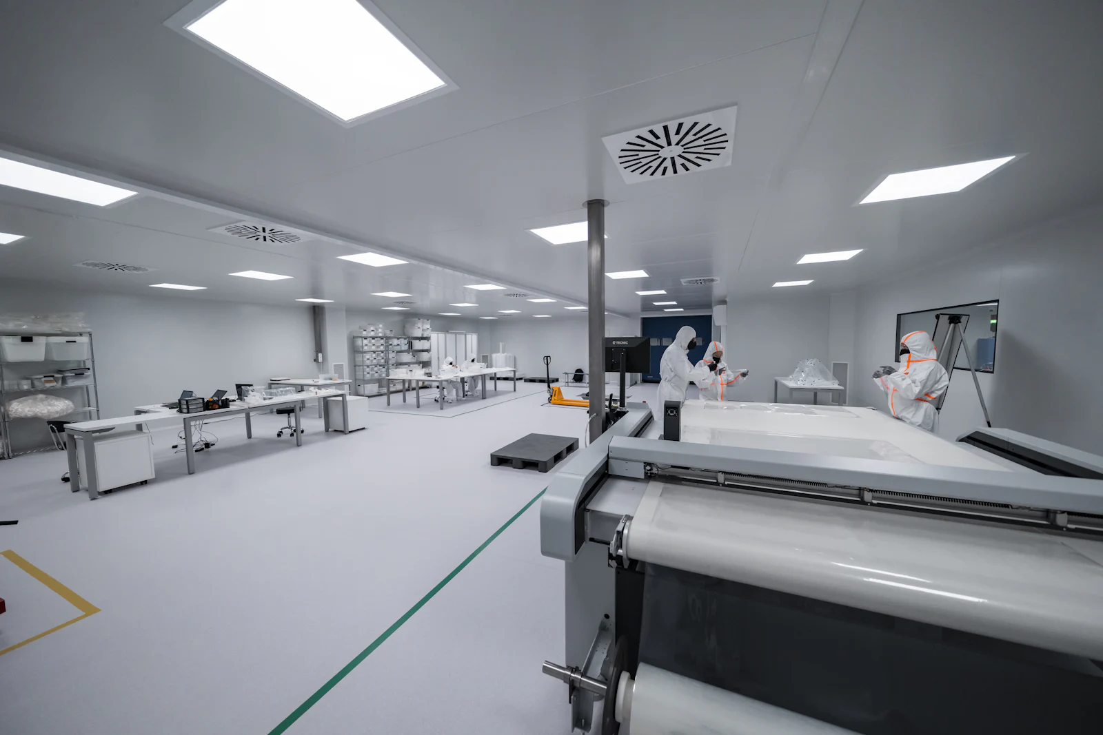
Who we are
India's independent partner for semiconductor quality and reliability
KAPSA Semicon provides advanced semiconductor testing, reliability, qualification, failure analysis and engineering services — giving chip designers, manufacturers and OEMs impartial, data-backed confidence in every device they ship.
- Independent and impartial — we test, we don't sell devices you compete with.
- Work aligned to JEDEC, AEC-Q100, MIL-STD and ISO/IEC 17025 practices.
- Engineering reports with root cause and recommendations — not just raw data.
What we do
End-to-end semiconductor engineering services
Eight specialist service areas, one accountable team — so your device moves from first silicon to qualified product without hand-offs between vendors.
Semiconductor Testing
Wafer, package, electrical, burn-in, parametric and production testing for ICs and discrete devices.
Learn more 02Reliability Engineering
JEDEC and AEC-Q100 qualification with environmental stress testing that proves long-term performance.
Learn more 03Failure Analysis
Non-destructive and destructive techniques to isolate defects and find the true root cause, fast.
Learn more 04Materials Characterization
Elemental, structural and chemical analysis of semiconductor and packaging materials.
Learn more 05Electronics Testing
PCB testing and failure analysis, EMC/EMI, functional and product qualification testing.
Learn more 06Calibration & Metrology
Traceable calibration of instruments and equipment used across semiconductor and electronics industries.
Learn more 07Semiconductor Packaging
Package design, assembly process development and package-level qualification for reliable devices.
Learn more 08Research & Development
Process development, reliability studies, new test methods and AI-based semiconductor analytics.
Learn moreFrom wafer to field
Support at every stage of the device lifecycle
Wherever your product is today — first silicon, qualification, production ramp or a field return — we plug in with the right tests and engineers.
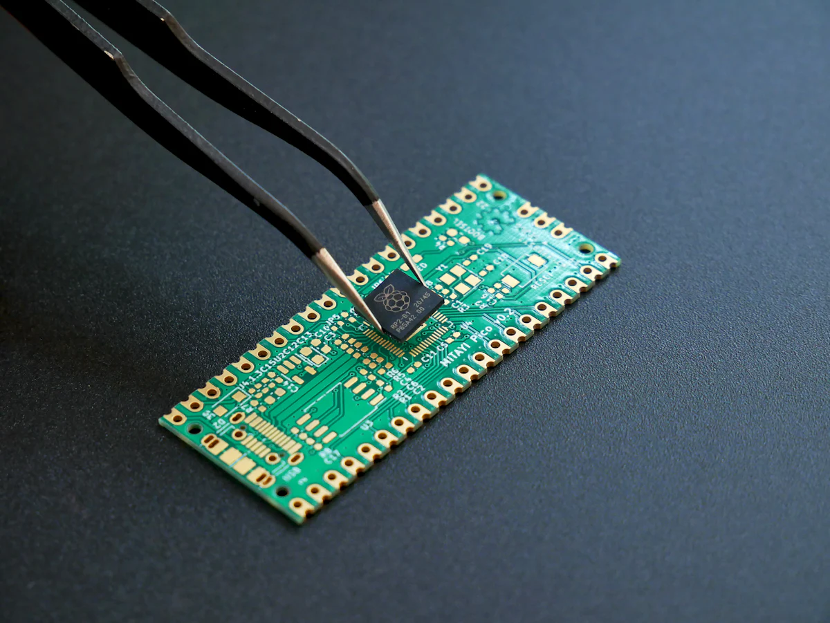
Design for reliability from day one
Package design reviews, material selection and early characterisation reduce the risk of late-stage qualification failures.
- Package design & assembly support
- Materials characterization
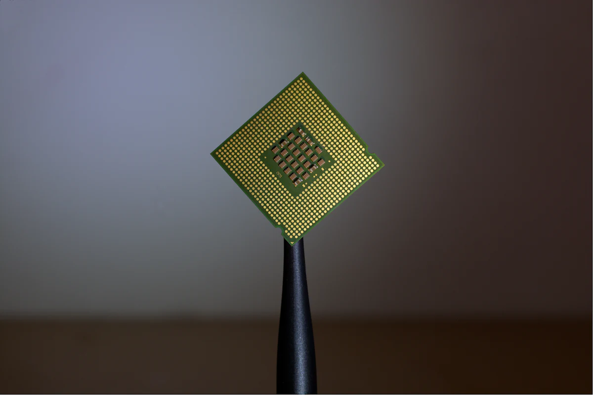
Electrical verification you can trust
Wafer-level and package-level electrical, parametric and functional testing to verify your design against specification.
- Wafer & package testing
- Parametric characterisation
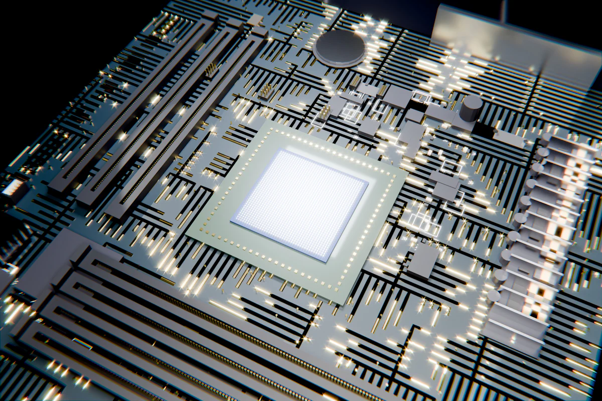
Qualify to the standard your market demands
Stress-test-driven qualification to JEDEC and AEC-Q100, with test plans built around your mission profile.
- HTOL, THB, HAST, temperature cycling
- HALT and environmental testing
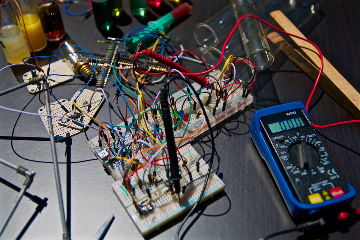
Ramp production with confidence
Production and burn-in testing screen out early-life failures, while board-level and EMC testing verify the end product.
- Burn-in & production test
- PCB, EMC/EMI & product qualification
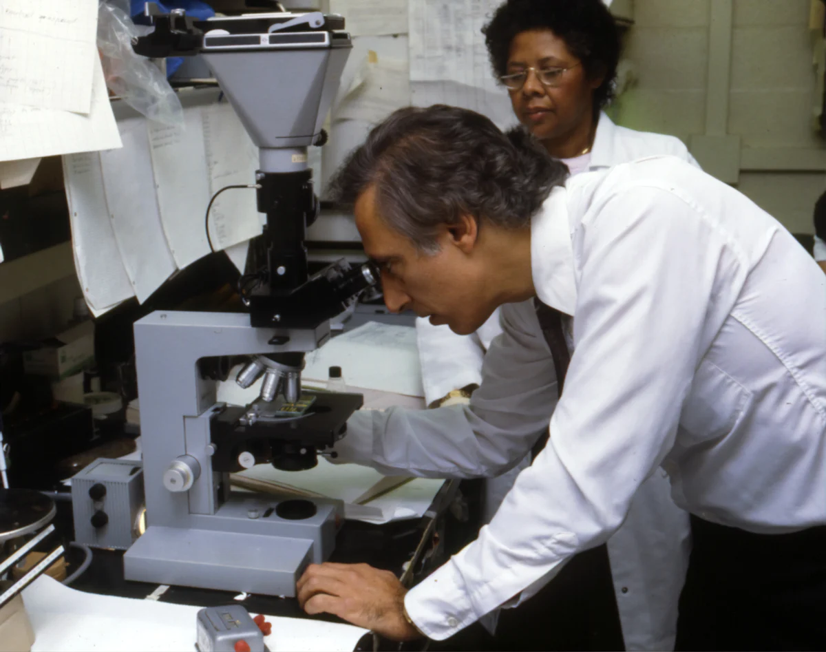
Find the root cause — and fix it
When something fails in qualification or in the field, our analysts isolate the defect and explain the mechanism behind it.
- X-ray, C-SAM, decapsulation
- SEM, FIB & cross-sectioning
Industries
Trusted where failure is not an option
We support teams building the devices that power vehicles, aircraft, hospitals, factories and national infrastructure.

Semiconductor
Fabless design houses, IDMs, foundries and OSATs needing independent test and qualification.

Automotive & EV
AEC-Q100 qualification for automotive and EV electronics.

Aerospace & Space
Screening and qualification for high-reliability applications.

Electronics & EMS
Board-level testing, EMC/EMI and product qualification for OEMs and EMS providers.

Defence
MIL-STD-aligned testing for mission-critical electronics.

Medical devices
Reliability evidence for life-critical electronics.

Industrial & energy
Robust electronics for harsh industrial environments.
Why KAPSA Semicon
Engineering rigour, delivered with speed
India's semiconductor ambitions need test capacity close to home. We combine global standards with local responsiveness, so you spend less time shipping samples abroad and more time shipping product.
Independent
Impartial results your customers and auditors can rely on.
Standards-driven
Test plans built on JEDEC, AEC, MIL-STD and IEC methods.
End-to-end
Testing, reliability and FA under one roof — no hand-offs.
Backed by KAPSA Global
Part of a group delivering engineering services since 2013.
Standards
Built around the standards your customers specify
Have a device, board or failure to investigate?
Share your requirement and our engineers will come back with a test plan, timeline and quotation — usually within one business day.